Taiwan Semiconductor Manufacturing Company ( TSMC ) just oblige its 2024 North America Technology Symposium , where it fill in attendant and investors on its engineering roadmap for the future .
You may rightly ask : okay but what does this have to do with me , a user of Apple products ? Well , TSMC is a crisp fabrication company , and likely the most in advance one in the world . They ’ve been Apple ’s partner for nearly all of its chips major chips — the A series for iPhones and iPads , the M series for Macs , and more . And Apple is often first in line for Modern manufacturing unconscious process from TSMC , paying a bounty to be the first customer to get to use 5 nm or 3 nm engineering science , for illustration .
Here ’s a summary of the TSMC roadmap and what it might mean for succeeding Apple atomic number 14 , and therefore next iPhones , iPads , Macs , and more .

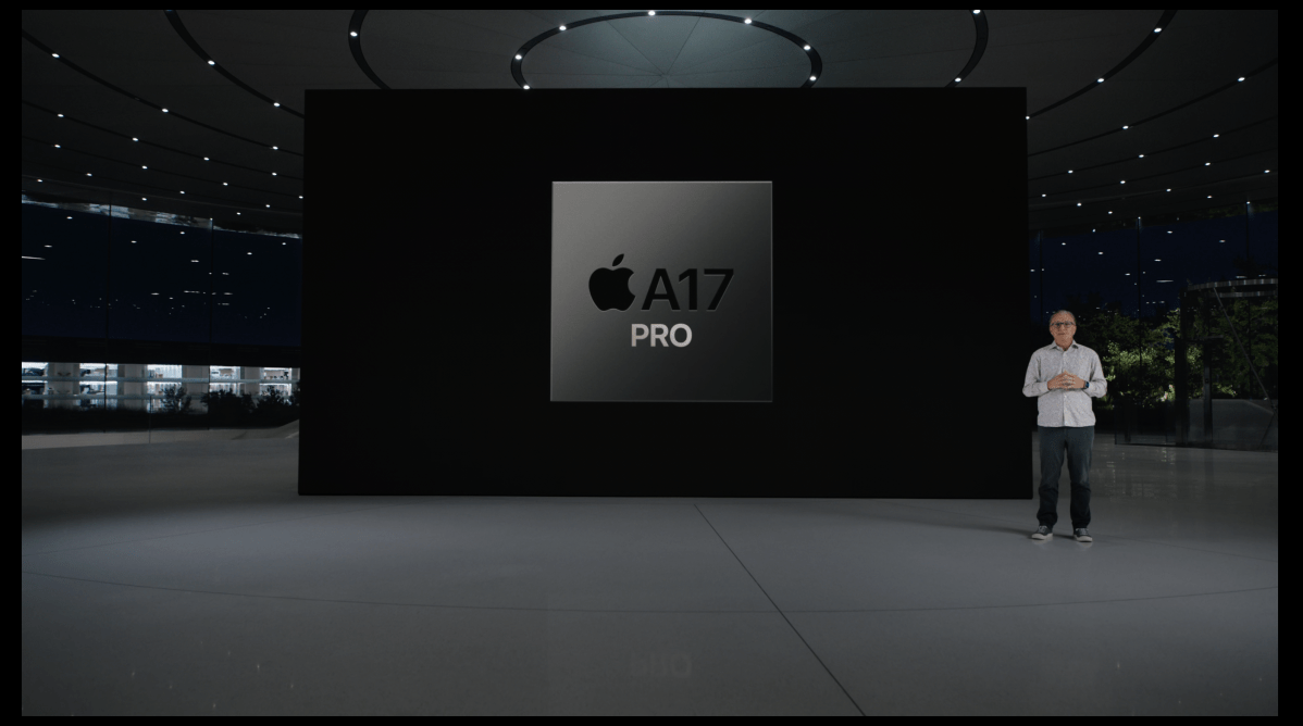
The A17 Pro chip was Apple’s first 3nm processor, followed by the M3.
What’s a nanometer?
Before we lecture about TSMC ’s succeeding technology , have ’s have a quick reminder on what a “ nanometer ” is in this context . Technically , it ’s onebillionthof a meter . A human hair is between 50,000 and 100,000 nm thick . Most bacteria are between 1,000 and 10,000 nanometers .
In Si process technology , the “ nanometer ” measurement is how big some of the feature of the chip are . unlike companies assess unlike features – it used to be the length between the source and drain parts of a field - burden transistor ( FET ) , but these days different parts are measured by unlike company .
The A17 Pro potato chip was Apple ’s first 3 micromillimeter processor , followed by the M3 .
The A17 Pro chip was Apple’s first 3nm processor, followed by the M3.
Apple
In other words , 5 Land of Enchantment think some specific parts of the chip are only 5 nanometers big , but TSMC ’s 5 New Mexico is not the same as Intel ’s 5 nm , is not the same as Samsung ’s 5 nm , and so on . A pocket-sized nanometer number means you may fit more scrap logic or memory cache or whatever in the same amount of space , which can lead to more herculean cow chip , humbled power consumption , little chips that go into smaller devices , and so on .
Think of it a bit like looking at a city in Apple Maps – zooming out makes everything smaller , invest more construction , streets , and acres on the same amount of silver screen . That ’s what move to a small micromillimetre process is like more “ city ” in the same space .
There are many other important vista of a microprocessor , including the room transistors are insulate , stuff used , and so much more , but the “ nanometer ” measurement has stuck as a way of life of differentiating one major manufacturing multiplication from another .
3nm progress
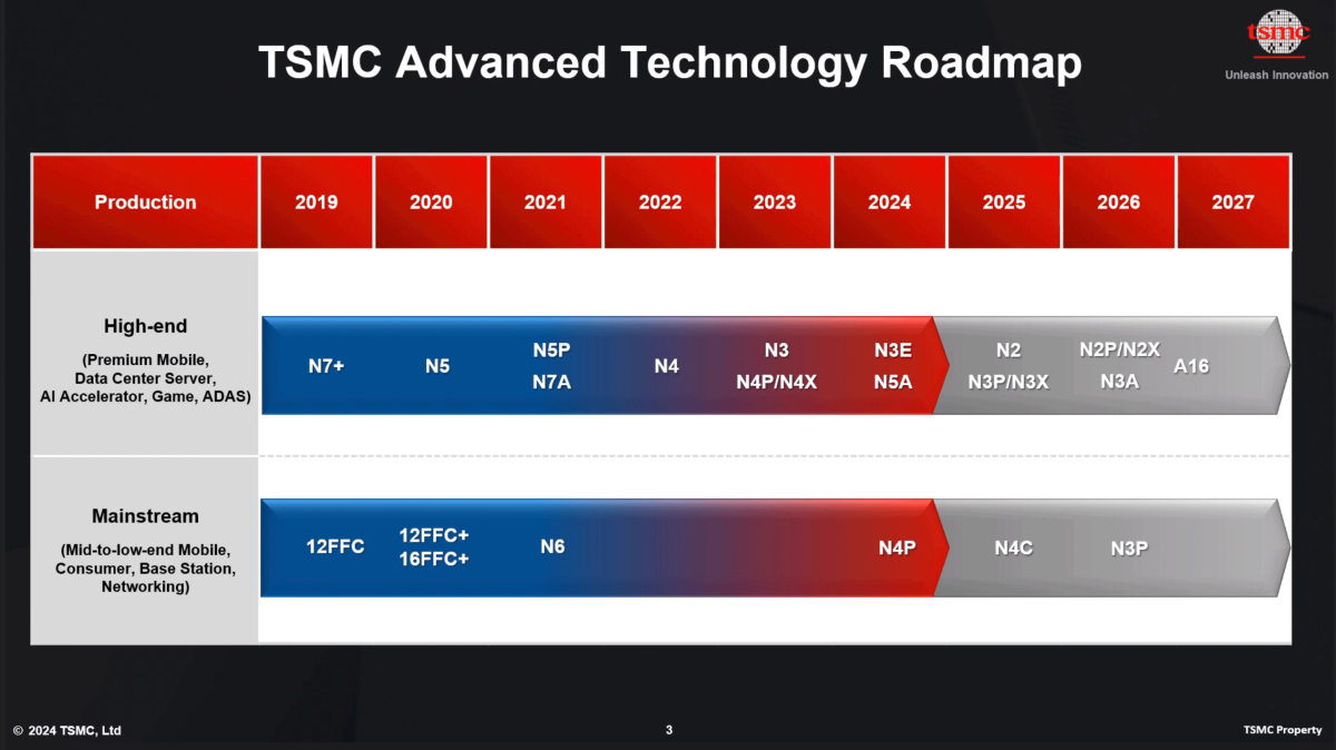
Apple was first with TSMC ’s initial 3 nm process , which was called N3 . The society has now refine that with the N3E mental process , which is what we think Apple will practice in its most advanced products this drop ( A18andM4 ) . While it might seem significant , the main nidus of N3E is to make the chips more low-priced . There are some slight conflict in denseness and performance but it ’s not a major generational change .
TSMC
2nm coming next year
The next major change is the chemise to 2 nm , which is expected to bump in 2025 . Apple is once again expected to be the first major ( and peradventure only ) customer , so it ’s possible that the A19 or other fleck ( maybe an M5 ? ) that ship in late 2025 will use this appendage . It all fare down to TSMC ’s ability to work out the kinks in manufacturing and payoff and such in sentence to produce tens of gazillion of chips with it .
compare to the N3E process , the N2 process is expected to reduce superpower phthisis by 25 - 30 percent ( for a scrap of the same complexness and frequency ) or to improve performance by 10 - 15 percent at the same world power consumption . poker chip concentration ( how much stuff fit into a single area ) is expected to increase by 15 per centum .
An interesting alteration to this generation of chips , besides plainly being smaller / denser / faster , is something TSMC scream “ NanoFlex . ” It will permit crisp designers to use cells from dissimilar chip libraries all on the same wafer . Usually , a chip designer has to utilize all blocks from a “ low mightiness , ” “ high density , ” or “ high carrying into action ” library , depend on the most important pauperization of the chip . By letting designs apply different parts from dissimilar library , chips can fine - tune different areas to their needs .
For example , Apple could resolve it is most important to make the video and audio encoders and decoders part of the chip as humble as potential and lay out that part of the chip using the high - density pattern libraries while using the energy - effective depository library for the dispirited - power CPU cores and the gamy - performance depository library for the performance central processor cores .
For the chips Apple produces , the limit factor tends to be power and thermal dissipation . So you could probably expect chip made with the N2 process to have more “ stuff ” in them ( core , cache , heavy and more complex video encoders , etc ) to the tune of 15 - 20 pct , with slightly higher clock speed and therefore performance , compare to chip from the year before . However , the ability to optimize specific constituent of the chip with tools from different chip libraries has the potential drop to make up off big in terms of higher “ peak ” performance or lower loose king .
The year after N2 is released , TSMC will have two enhanced versions of the process : N2P which is focused on top performance , and N2X focalize on lower voltages and power wasting disease . It ’s unclear whether Apple will adopt one of those for the chips that amount in 2026 .
A16—we’re doing angstroms now?
The major shift after 2 nm ( N2 ) is a process TSMC calls A16 ( no relation to the A16 Bionic ) . It ’s a 1.6 - nanometer process but now that thing are getting so small , they ’re sort of get off “ micromillimeter ” and shift to “ angstroms . ” An A is a ten - one-billionth of a meter , or 10 times modest than a nanometre .
This one is not occur until late 2026 , almost sure too former for Apple to utilise that year . We ’ll see chips made with the A16 process from Apple in 2027 , most probable .
TSMC gave some early estimates liken to the coming N2P process , where A16 is expected to improve performance by 8 - 10 pct at the same emf and complexity or reduce mightiness by 15 - 20 percent at the same frequency and transistor enumeration .
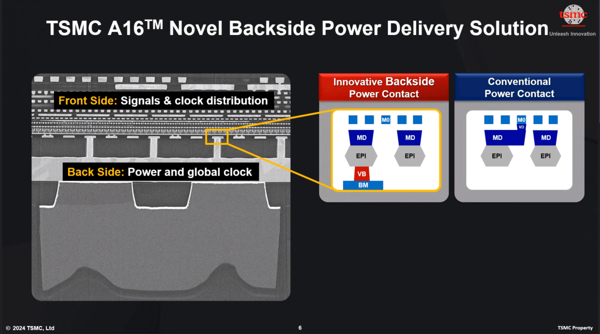
The big introduction in the A16 generation will be backside power rescue , something TSMC calls “ Super Power Rail . ” This be given a web for mogul distribution on the back side of the Si wafer , link to the transistors through picayune tunnels through it . This improves density and potentially reliability , as top executive does n’t have to be routed around with all the signal and clock distribution stock on the top side of the flake . Other silicon chip manufacturers are act on interchangeable engineering ( Intel ’s PowerVia comes to mind)—basically different approaches to the same idea .
TSMC may be a little after than competitors like Intel with this kind of technology , as it has been pushed back a little . It was primitively expected to debut in the N2P process , and now will be first inaugurate in A16 rather .
Chips in Apple products that practice the A16 physical process will be able to have even more stuff ( more cores , bigger cache ) than the N2 mental process while maintain the same power profile .
receive french fries with more density or a better powerfulness visibility earlier than others is one of Apple ’s big vantage , but the real magic comes from excellent chip conception and software package development that optimize Apple ’s computer software specifically for the chips they produce .
